
What is a Blind Via in HDI PCB?
In the world of printed circuit boards (PCBs), HDI PCBs (High-Density Interconnector PCBs) have revolutionized the design and manufacturing of modern electronic devices. One of the critical features of HDI PCBs is the use of various types of vias, which help in creating interconnections between different layers of the board. Among these, the blind via stands out due to its specific functionality and application.
Understanding Blind Vias in HDI PCBs
A blind via in HDI PCB refers to a via that connects an outer layer of the PCB to one or more inner layers but does not extend all the way through the entire board. Unlike through-hole vias, which go through the whole thickness of the PCB, blind vias only make connections from an external layer to an internal layer, with the via hole remaining closed at the opposite end.
This design choice is crucial for creating high-density boards where space is limited, and the need for more efficient routing of electrical signals is essential. The main benefit of using blind vias is that they help conserve space and allow for more complex routing on HDI PCBs. By limiting the via to only certain layers, designers can achieve a compact layout that accommodates more components and interconnections.
Benefits of Using Blind Vias in HDI PCBs
Space Efficiency: Blind vias allow for better space utilization by eliminating the need for through-hole vias that take up space on both sides of the PCB. This is particularly important for hdi pcb, which are designed to be smaller, lighter, and more compact, often used in smartphones, laptops, and other high-tech gadgets. Higher Density: The use of blind vias supports higher component density by enabling designers to create multi-layered boards without taking up valuable space. This makes HDI PCBs ideal for devices requiring a high number of connections in a small area.
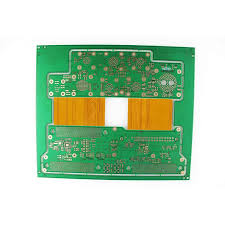
Improved Signal Integrity: Blind vias can help reduce signal loss and interference, a critical concern in high-speed electronics. By strategically placing blind vias, manufacturers can optimize the electrical performance of the HDI PCB. Cost-Effective Manufacturing: Although HDI PCB designs are typically more expensive to produce due to their complexity, the use of blind vias can reduce the overall cost by minimizing the number of layers required, making the design more affordable to manufacture.
Types of Vias in HDI PCBs
While blind vias are a crucial element in HDI PCBs, it’s important to differentiate them from other types of vias used in PCB design: Through-Hole Vias: These vias run from one side of the PCB to the other, making connections between all layers of the board. While these are simpler and less costly to manufacture, they do not offer the space-saving benefits of blind vias.
Buried Vias: Buried vias are entirely contained within the inner layers of the PCB. They do not connect to the outer layers, unlike blind vias, and are used for more specialized routing applications within HDI PCBs. Micro-Vias: Micro-vias are extremely small vias used in high-density designs. Blind vias can be micro-vias when they are drilled with smaller diameters to accommodate more precise connections within HDI PCBs.
Conclusion
In conclusion, blind vias play a pivotal role in the design of HDI PCBs, providing an efficient method for routing electrical signals while optimizing space and improving overall performance. By incorporating blind vias, manufacturers can create compact, high-performance circuit boards that meet the demands of modern electronics, all while enhancing signal integrity and reducing the cost of production. For engineers working on HDI PCBs, understanding the benefits and functionality of blind vias is crucial to achieving the most efficient and cost-effective designs.