
manufacture multilayer RF circuit boards
Manufacturing multilayer RF (Radio Frequency) circuit boards is a complex and highly specialized process that requires precision and advanced techniques. These circuit boards are crucial for a wide range of applications, including telecommunications, satellite systems, medical devices, and automotive electronics, where high-frequency signals need to be processed with minimal loss and interference. Multilayer RF circuit boards consist of multiple layers of conductive and insulating materials, enabling the integration of complex circuits into a compact form factor. The process of manufacturing these boards involves several stages, including design, material selection, lamination, etching, and testing.
The first step in manufacturing multilayer rf circuit board is designing the layout. This involves using specialized software, such as CAD (Computer-Aided Design) tools, to create detailed designs of the circuit board. The design must take into account the specific requirements for RF performance, such as impedance control, signal integrity, and minimizing electromagnetic interference (EMI). The layout typically involves the placement of components such as antennas, capacitors, resistors, and inductors across multiple layers. In multilayer RF boards, the design also ensures that signal traces are routed in a way that optimizes the board’s performance and minimizes losses at high frequencies.
Once the design is complete, the next step is selecting the materials. RF circuit boards require specialized materials with low dielectric constants and low loss tangents to ensure minimal signal degradation. Materials such as PTFE (polytetrafluoroethylene), Rogers, and other high-frequency laminates are commonly used. These materials help maintain the integrity of the RF signals as they travel through the circuit board. The choice of material depends on the frequency range of the application, as different materials perform better at different frequencies. The core material is usually a thin sheet of copper-clad laminate, which is then coated with an insulating layer that provides electrical isolation between the conductive layers.
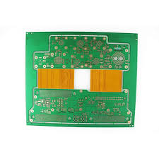
How do you manufacture multilayer RF circuit boards?
The next stage in the process is the lamination of the layers. Lamination involves bonding multiple layers of the copper-clad laminate and insulating material to create a solid, multilayer structure. The layers are stacked and subjected to high pressure and temperature in a vacuum press. This process ensures that the layers are tightly bonded together and that the insulation between the layers is uniform. The number of layers in the board can vary depending on the complexity of the design, with some RF circuit boards having as many as 12 layers or more. After lamination, the multilayer structure is cooled and prepared for the next steps.
After lamination, the circuit board undergoes etching to define the conductive traces and patterns. Etching removes the unwanted copper from the board, leaving behind the desired signal pathways. This is typically done using a chemical process, where the copper is exposed to an etching solution that dissolves the excess copper. The etching process must be extremely precise, as even small errors can impact the board’s performance. In RF circuit boards, the etching process is particularly critical for controlling the impedance of the traces, as variations in impedance can lead to signal loss and reflection.
Next, vias are drilled into the multilayer circuit board to create electrical connections between the layers. These vias allow signals to pass from one layer to another, ensuring that the circuit board functions as intended. There are several types of vias, including through-hole vias, blind vias, and buried vias, each serving a different purpose depending on the design of the board. The vias are typically filled and plated with copper to ensure a solid electrical connection between the layers.
After drilling and via plating, the board undergoes a series of tests to ensure it meets the required specifications. These tests may include electrical testing to check for continuity and short circuits, as well as RF performance testing to measure the signal loss and impedance of the board. In some cases, the board is also subjected to environmental testing, such as temperature cycling or humidity tests, to ensure it will perform reliably in real-world conditions.
Finally, the completed multilayer RF circuit boards are packaged and ready for assembly. Components are soldered onto the board using surface-mount technology (SMT) or through-hole soldering, depending on the design. The finished boards are then subjected to further testing to ensure they function correctly in their intended applications.