
Proper Signal Integrity in Rigid Flex PCB Designs
Rigid-flex circuits offer many benefits to PCB designers, including allowing for greater mechanical stability and flexibility in a smaller package. However, these circuits have unique requirements that need to be addressed during the design process in order to guarantee optimal performance and durability. A rigid-flex circuit’s layer stack up, the arrangement of copper and dielectric materials, and the positioning of connectors all play a role in signal integrity. To minimize noise and jitter, it is important to ensure that these circuits are properly grounded to reduce electromagnetic interference (EMI) and maintain proper impedance. In addition, the material selection process needs to account for varying thermal expansion properties between the rigid and flexible sections of the board.
The minimum bend radius of a rigid flex pcb is crucial to the reliability of the design. Without a sufficient radius, the flex section will become strained and prone to cracking and failure over time. This is why it is vital to consult the IPC-2223B standard when determining the minimum bend radius for your design.
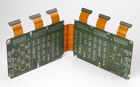
It is also important to pay attention to the layout of pads, holes, and vias in a rigid-flex design. Placing plated holes, vias, or pads in areas that are subject to bending can apply mechanical stress and potentially tear them or the structure of a flex circuit’s traces. To avoid these issues, it is best to place all plated holes, vias, or pads on the rigid section of the circuit or in areas that are not subjected to bending.
How to Ensure Proper Signal Integrity in Rigid Flex PCB Designs
When routing a flex circuit, it is a good idea to stagger the traces rather than having them overlap each other. This can help to spread the load on the conductors and prevent them from becoming damaged or broken over time, which will increase overall durability and reliability.
Insufficient hole-to-flex spacing can cause mechanical stress concentration and tearing in the flex section, which will negatively impact signal integrity and solder joint reliability. To ensure the integrity of the flex to rigid transition, it is important that this space be greater than 50 mil.
The use of blind and buried vias in a rigid-flex circuit can also cause problems. These vias can create unwanted connections, which will lead to noise and jitter in the signal path. To avoid these issues, it is best not to use these types of vias in a flex section and to instead use through-hole or microvias.
Achieving proper signal integrity in a rigid-flex PCB requires careful planning and consideration of all of the above factors. Keeping these tips in mind will allow you to design the best possible rigid-flex circuit, and it will also help you ensure that your rigid-flex PCB meets industry standards for quality and reliability. To learn more about rigid-flex technology or to get started designing your own, contact a professional rigid-flex PCB manufacturer today. They can provide the expertise and tools needed to design and fabricate your project quickly and effectively. They can also implement sound shielding and grounding methodologies to mitigate EMI and improve signal integrity.