
Via in Pad in High-Density Electronics
“Via in Pad” is a prominent technique in printed circuit board (PCB) design that has revolutionized how high-density and compact electronics are created. This technology involves placing vias directly under or within the pads of surface-mounted components, enhancing both the electrical and thermal performance of PCBs. Widely adopted in modern designs, especially for high-frequency and high-speed applications, “Via in Pad” helps address the challenges posed by miniaturization and increasing complexity in electronic devices.
Traditionally, vias were positioned outside component pads to connect different layers of a PCB. While effective, this approach often required more space and could complicate routing in densely packed boards. The “Via in Pad” technique resolves these issues by integrating the via into the pad itself. This innovation allows for closer placement of components, better thermal dissipation, and reduced signal interference. As a result, it has become indispensable in the design of compact devices such as smartphones, wearable technology, and advanced medical instruments.
One of the most significant advantages of “Via in Pad” is its contribution to signal integrity. In high-frequency designs, minimizing the distance between components is crucial to reducing signal loss and maintaining performance. By placing the via directly within the pad, designers can shorten trace lengths, which helps to preserve signal quality. This feature is particularly important in applications like 5G communication systems and advanced computing, where even minute signal disruptions can have a significant impact.
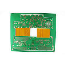
The Role of Via in Pad in High-Density Electronics
Thermal management is another area where “via in pad” excels. Electronic components generate heat during operation, and efficient thermal dissipation is essential to maintaining their reliability and lifespan. With vias integrated into pads, heat can be efficiently transferred through the PCB layers to thermal planes or heat sinks. This design eliminates the need for additional thermal management solutions, reducing overall system complexity and cost.
Despite its many benefits, implementing “Via in Pad” technology comes with challenges. One of the primary concerns is the risk of solder voids during the assembly process. When solder paste flows into the via, it can create air pockets that weaken the solder joint. To address this, manufacturers use techniques such as plugging, capping, or filling the vias with conductive or non-conductive materials. These methods ensure reliable connections and prevent solder wicking.
The cost of manufacturing PCBs with “Via in Pad” can also be higher than traditional designs due to the advanced fabrication processes involved. However, the long-term advantages, including enhanced performance and reduced form factor, often justify the initial expense for high-end applications.
In summary, “Via in Pad” technology is a game-changer in PCB design, providing solutions to challenges in high-density and high-performance electronics. Its ability to improve signal integrity, enhance thermal performance, and optimize board layout has made it a go-to choice for engineers tackling modern design requirements. While it requires careful planning and advanced manufacturing techniques, the benefits of this innovative approach far outweigh its complexities, paving the way for the next generation of electronic devices.