
PCB Fabrication and Assembly Affect Signal Integrity
PCBs are essential in electronic devices and systems, providing the necessary foundation for component placement and signal transmission. However, a multitude of factors can degrade the transmission integrity of the data on a PCB, impacting the overall quality and functionality of the finished product. It is important to understand how these factors affect signal integrity and what can be done to mitigate them.
PCB fabrication begins with the design process, using CAD and other software programs to create a circuit board layout including components and their locations on the circuit board. Once the layout is finalized, the CAD files are sent to a company that specializes in PCB assembly and manufacturing. They will perform a series of checks called “design for manufacturability” or DFM, to ensure the PCB meets all the design specifications.
Once the pcb fabrication assembly is ready to be assembled, a mixture of solder alloy and flux called solder paste is applied to designated areas on the circuit board, known as pads. The resulting solder is then subjected to a reflow process, where heat is applied to melt the solder and create reliable electrical connections. Component Placement: Automated machines known as pick-and-place machines accurately place surface-mount components onto the populated PCB. This is a time-saving and labor-efficient method of assembling high volumes of PCBs.
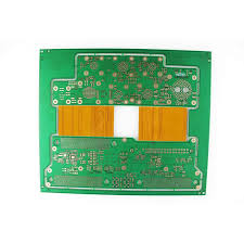
How Do PCB Fabrication and Assembly Affect Signal Integrity?
Visual Inspection: A careful visual inspection of the completed PCB is conducted to ensure it is free of any defects or irregularities. This step is especially important for high-speed circuit boards, where any anomalies could significantly impact signal integrity.
DFM: Design for Manufacturability: When a circuit board is designed for high-speed digital or analog topologies, it should follow a set of rules and guidelines known as “design for manufacturability,” or DFM. These guidelines will determine things like trace width and spacing requirements for different signal types, differential pairs, and power and ground needs. In addition, they will dictate the specific layer stack-ups required for each of these signals, as well as how to deal with common issues like crosstalk and switching noise.
Printed Circuit Board Assembly: A variety of processes take place during the assembly and manufacturing of a PCB, all of which can affect its signal integrity. For example, during lamination, mechanical stress on the PCB can cause alignment tolerances to skew and alter impedance values, which could lead to signal reflections. Strict adherence to alignment tolerances is critical for maintaining signal integrity. Other process variables, such as imaging, etching, and plating can also cause variations in trace geometry and impedance, but careful and consistent process optimization can reduce these effects.
Another potential issue with signal integrity is excessive crosstalk, which occurs when a high-speed signal on one trace couples to the return path plane of another adjacent signal. This can cause the victim signal to acquire the characteristics of the aggressor signal and can lead to unwanted interference. To avoid this, a good rule of thumb is to maintain a distance between sensitive traces that is at least three times their width.