
microvia differ
Printed circuit boards (PCBs) with microvias have greater electrical performance than conventional rigid PCBs and are more flexible. In addition, they can also reduce the amount of manual routing required to connect components and traces. Microvias are small holes in a PCB that allow the copper layers to connect. During the manufacturing process, pure copper or an epoxy with copper resin is placed into these holes to connect inner-layer circuits to the PCB surface. The microvia holes can be stacked or staggered, which offers different benefits to the board designer.
Stacked microvias line up one on top of another from layer to layer, which closely resembles the structure of a traditional through-hole via. Staggered microvias offer a similar design, but with the added benefit of allowing traces to move in the x- and y-planes between layer transition points. This can help improve power and ground plane performance by reducing choke points and increasing signal transmission speed.
Both types of microvia can be fabricated using laser drilling and photo imaging technology. Laser drilling yields the smallest and densest microvia structures, while photoimaging offers reduced costs where ultra-fine features are not necessary. Both technologies employ stringent fabrication processes and rigorous quality assurance measures to ensure that the microvia holes are free of debris, plating failures, and other defects that can lead to reliability issues.
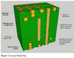
How do microvia differ from traditional rigid PCBs?
During laser drilling, a microvia hole requires precise energy pulses to maintain tight tolerances across multiple layers. In order to do this, the laser must be highly accurate, delivering very thin conformal seed layers inside each microvia hole. This allows for the subsequent copper electroplating steps to deposit a thicker layer of metal until the via body is filled with solid, void-free copper. To achieve this, statistical process controls must be in place to measure microvia diameters, capture pad sizes and depth uniformity, driving the metallization process towards 6 sigma capability levels or better.
One of the biggest challenges with fabricated microvias is debris-based interconnect defects (ICDs). These occur when particles or debris make their way through the via and into the inner copper layer, leading to short circuits, open circuits, and intermittent problems under high temperatures. To reduce the risk of ICDs, a manufacturer should thoroughly clear all microvia holes of drill smear, residue, fiberglass, inorganic fillers and other material before filling them with copper.
A faulty copper wrap plating can be the culprit of these ICDs, and this is common in simple, stacked microvia designs. The condition usually manifests as a short at the bottom of one microvia and a metallurgical connection with the adjacent copper layer or the microvia walls. This has been observed in IPC test boards with stacked microvias and has led to an IPC test committee established to study the problem in more detail. However, this problem has not been reported in staggered microvias. Moreover, the problem appears to be more of an issue with the thickness of the copper wrap plating rather than its location on the surface of the microvia or in the metallurgical junction between the through-hole and the microvia walls.